Dual Core Microcontroller
The Ensemble E3 series of microcontroller is designed for applications demanding a combination of maximum power efficiency, high compute performance, and integrated security. It’s innovative multi-code design provides a dedicated system for power efficient operations, while the second core is ready to deliver high-performance processing when needed. Both cores can also be outfitted with dedicated NPU accelerators to boost Edge AI/ML capabilities and can operate independent of each other, enabling parallel model execution.
Key Benefits of E3:
-
High-Performance RTOS control and AI/ML (Artificial Intelligence/Machine Learning)
-
Low-power MCU/NPU wakes system
-
User interface and networking
E3 Specifications
- High-Performance Arm® Cortex®-M55 Core, up to 400 MHz, with Helium™ Vector Processing Extension, Double-Precision FPU, 1.25MB SRAM 0-wait State Tightly- Coupled Memory, 32KB Instruction and Data Caches, Armv8.1-M ISA with Arm TrustZone®, and 4.37 CoreMark®/MHz Performance Benchmark
- Arm® Cortex®-M55 Core, up to 160 MHz, with Helium™ Vector Processing Extension, DoublePrecision FPU, 512KB of SRAM 0-wait State Tightly Coupled Memory, 32KB Instruction and Data Caches, Armv8.1-M ISA with Arm TrustZone®, and 4.37 CoreMark®/MHz Performance Benchmark
- High-Performance 400-MHz 64-bit AXI Bus Fabric Common Across All CPUs
- 2× Arm Ethos™-U55 Neural Processing Units— 1× 256 MAC/cycle up to 204 GOPS, 1× 128 MAC/cycle up to 46 GOPS, On-the-Fly Weight Decompression with Dedicated DMA Controller
- 800× Performance Uplift from Cortex-M4 for Inference Time (Source: Arm. MobileNet V2 1.0 Model for Object Classification)
- 76× Less Energy Consumed when Using Ethos-U55 together with Cortex-M55 (Source: Arm. Measured on Alif Semiconductor Ensemble Device. MobileNet V2 1.0 Model for Object Classification)
- Autonomous Intelligent Power Management (aiPM™)
- FD-SOI Low Leakage Process
- 1.7 µA Consumed in STOP Mode with LPRTC, LPTIMER, LPCMP, BOR, 4KB Utility SRAM, Wake Pins
- As Low as 27 µA/MHz Dynamic Consumption for High-Efficiency Cortex-M55
- Multiple Power Domains, Dynamic Power, Gating, Voltage and Clock Scaling, DC-DC Converter
- High Endurance MRAM Non-Volatile Memory
- Up to 5.5MB
- SRAM
- Up to 13.5MB
- Optional Data Retention of 256KB or 512KB TCM SRAM Consuming 2.25 μA or 4.5 μA
- 4KB Always-On Utility SRAM
- 2× Octal SPI, each at up to 100 MHz for up to 100 MB/s SDR, 200 MB/s DDR, with Inline AES Decryption, XIP Mode Support, HyperBus Protocol Support, Enabling External Memory Expansion
- 1× SD® v4.2, eMMC™ v5.1 Channel with DMA
- Hardware-based Root-of-Trust (RoT) with Unique Device ID
- Secure Key Generation and Storage, Secure Certificate Storage
- Factory-provisioned Private Keys
- Crypto Accelerators—AES (up to AES-256), ECC (up to 384 bits), SHA (up to SHA-256), RSA (up to RSA-3072), and NIST compliant TRNG
- Secure Debugging with Certificate Authentication
- 12× Universal High-Resolution 32-bit Timers
- Capable of Motor and LED Lighting Control
- 2× Watchdog Timers
- 4× Low-Power 32-bit Timers
- 1× Real-Time Counter
- 4× Quadrature Encoder Counters
- 1× 10/100 Ethernet with DMA
- 1× USB 2.0 HS/FS Host/Device with DMA
- 1× SDIO v4.1 Channel with DMA
- 1× CAN FD Channel up to 10 Mbps
- 1× MIPI® I3C® Channel
- 4× I2C Channels up to 3.4 Mbps Throughput
- 1× Low-Power I2C Channel
- 8× UART Channels up to 2.5 Mbps (4× with RS485 Driver Control)
- 1× Low-Power UART Channel
- 4× SPI Channels up to 50 Mbps Throughput
- 1× Low-Power SPI Channel
- 3× 12-bit ADC (18 Single-Ended Inputs)
- 1× 24-bit ADC (4 Differential Inputs)
- Programmable Gain Instrumentation Amplifier (1× to 128×)
- 2× 12-bit DACs (2 channels)
- 4× High-Speed Analog Comparators with 2.5-ns Response (16 Inputs)
- 1× Low-Power Analog Comparator (4 Inputs)
- Internal Temperature Sensor
- Internal Precision Reference Voltage
- 1× 2-Lane MIPI CSI-2®
- 1× Camera Parallel Interface (CPI), up to 16 bits
- 1× Low-Power CPI, up to 8 bits
- Graphics LCD Controller
- 1× Display Parallel Interface (DPI), up to 24-bit RGB
- 1× 2-Lane MIPI DSI®
- D/AVE 2D Graphics Processing Unit
- 4× I2S Synchronous Stereo Audio Interfaces
- 1× Low-Power I2S Stereo Audio Interface
- 4× 2-channel Pulse Density Modulation (PDM) Microphone Inputs (8 Mono Microphones)
- 4× 2-channel Low-Power Pulse Density Modulation (LPPDM) Microphone Inputs (8 Mono Microphones)
- Up to 120× 1.8-V GPIOs (Shared with Peripherals)
- Up to 8× Selectable 1.8-V to 3.3-V GPIOs (Shared with Peripherals)
- Internal Low-Frequency RC Oscillator (32.7 kHz, ±4%)
- Internal High-Frequency RC Oscillator (Up to 76.8 MHz, ±1%)
- External High-Frequency Crystal Oscillator or Quartz Crystal (24 MHz to 38.4 MHz)
- External Low-Power Crystal Oscillator or Quartz Crystal (32.768 kHz)
- One User Fractional Mode PLL
- Global Event Mapping to Configurable Triggers
- 3× 32-Channel General DMA Controllers
- CRC Calculation Accelerator with Programmable Polynomials
- Programmable Low Supply Voltage Detect Warning (Brown-Out Detect)
- Power-On Reset and Brown Out Reset
- Real-Time Clock
- JTAG/SWD Debug Interface
- 1.75 V to 4.2 V Primary Supply Range
- 1.08 V to 1.98 V I/O Supply Range (1.8 V I/O)
- 3.0 V to 4.2 V I/O Supply Range (3.3 V Flex I/O)
- -40 °C to 85 °C Extended Ambient Temperature Range
- -40 °C to 125 °C Extended Junction Temperature Range
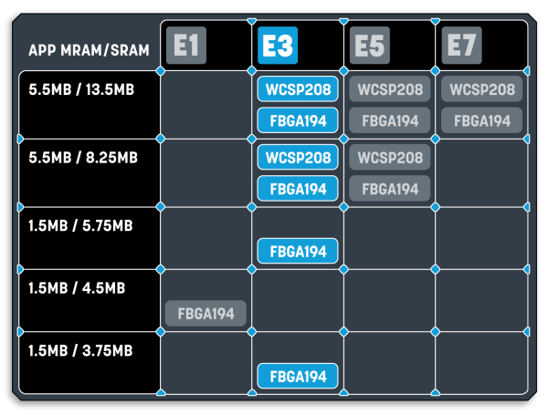
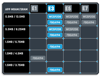
- WLCSP208, 0.5 mm Pitch
- FBGA194, 0.5 mm Pitch
High-Performance Dual-Core MCU
- High-Performance Arm® Cortex®-M55 Core, up to 400 MHz, with Helium™ Vector Processing Extension, Double-Precision FPU, 1.25MB SRAM 0-wait State Tightly- Coupled Memory, 32KB Instruction and Data Caches, Armv8.1-M ISA with Arm TrustZone®, and 4.37 CoreMark®/MHz Performance Benchmark
- Arm® Cortex®-M55 Core, up to 160 MHz, with Helium™ Vector Processing Extension, DoublePrecision FPU, 512KB of SRAM 0-wait State Tightly Coupled Memory, 32KB Instruction and Data Caches, Armv8.1-M ISA with Arm TrustZone®, and 4.37 CoreMark®/MHz Performance Benchmark
- High-Performance 400-MHz 64-bit AXI Bus Fabric Common Across All CPUs
Efficient Micro NPUs for AI/ML Acceleration
- 2× Arm Ethos™-U55 Neural Processing Units— 1× 256 MAC/cycle up to 204 GOPS, 1× 128 MAC/cycle up to 46 GOPS, On-the-Fly Weight Decompression with Dedicated DMA Controller
- 800× Performance Uplift from Cortex-M4 for Inference Time (Source: Arm. MobileNet V2 1.0 Model for Object Classification)
- 76× Less Energy Consumed when Using Ethos-U55 together with Cortex-M55 (Source: Arm. Measured on Alif Semiconductor Ensemble Device. MobileNet V2 1.0 Model for Object Classification)
Extreme-Low Power Technology
- Autonomous Intelligent Power Management (aiPM™)
- FD-SOI Low Leakage Process
- 1.7 µA Consumed in STOP Mode with LPRTC, LPTIMER, LPCMP, BOR, 4KB Utility SRAM, Wake Pins
- As Low as 27 µA/MHz Dynamic Consumption for High-Efficiency Cortex-M55
- Multiple Power Domains, Dynamic Power, Gating, Voltage and Clock Scaling, DC-DC Converter
On-Chip Application Memory
- High Endurance MRAM Non-Volatile Memory
- Up to 5.5MB
- SRAM
- Up to 13.5MB
- Optional Data Retention of 256KB or 512KB TCM SRAM Consuming 2.25 μA or 4.5 μA
- 4KB Always-On Utility SRAM
External Memory Interfaces
- 2× Octal SPI, each at up to 100 MHz for up to 100 MB/s SDR, 200 MB/s DDR, with Inline AES Decryption, XIP Mode Support, HyperBus Protocol Support, Enabling External Memory Expansion
- 1× SD® v4.2, eMMC™ v5.1 Channel with DMA
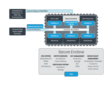
Secure Enclave
- Hardware-based Root-of-Trust (RoT) with Unique Device ID
- Secure Key Generation and Storage, Secure Certificate Storage
- Factory-provisioned Private Keys
- Crypto Accelerators—AES (up to AES-256), ECC (up to 384 bits), SHA (up to SHA-256), RSA (up to RSA-3072), and NIST compliant TRNG
- Secure Debugging with Certificate Authentication

Timing Control and Measurement
- 12× Universal High-Resolution 32-bit Timers
- Capable of Motor and LED Lighting Control
- 2× Watchdog Timers
- 4× Low-Power 32-bit Timers
- 1× Real-Time Counter
- 4× Quadrature Encoder Counters
Serial Communication Interfaces
- 1× 10/100 Ethernet with DMA
- 1× USB 2.0 HS/FS Host/Device with DMA
- 1× SDIO v4.1 Channel with DMA
- 1× CAN FD Channel up to 10 Mbps
- 1× MIPI® I3C® Channel
- 4× I2C Channels up to 3.4 Mbps Throughput
- 1× Low-Power I2C Channel
- 8× UART Channels up to 2.5 Mbps (4× with RS485 Driver Control)
- 1× Low-Power UART Channel
- 4× SPI Channels up to 50 Mbps Throughput
- 1× Low-Power SPI Channel
Analog Interface Capabilities
- 3× 12-bit ADC (18 Single-Ended Inputs)
- 1× 24-bit ADC (4 Differential Inputs)
- Programmable Gain Instrumentation Amplifier (1× to 128×)
- 2× 12-bit DACs (2 channels)
- 4× High-Speed Analog Comparators with 2.5-ns Response (16 Inputs)
- 1× Low-Power Analog Comparator (4 Inputs)
- Internal Temperature Sensor
- Internal Precision Reference Voltage
Camera Interfaces
- 1× 2-Lane MIPI CSI-2®
- 1× Camera Parallel Interface (CPI), up to 16 bits
- 1× Low-Power CPI, up to 8 bits
Display Interfaces & Graphics
- Graphics LCD Controller
- 1× Display Parallel Interface (DPI), up to 24-bit RGB
- 1× 2-Lane MIPI DSI®
- D/AVE 2D Graphics Processing Unit
Audio Interfaces
- 4× I2S Synchronous Stereo Audio Interfaces
- 1× Low-Power I2S Stereo Audio Interface
- 4× 2-channel Pulse Density Modulation (PDM) Microphone Inputs (8 Mono Microphones)
- 4× 2-channel Low-Power Pulse Density Modulation (LPPDM) Microphone Inputs (8 Mono Microphones)
General Input/Output
- Up to 120× 1.8-V GPIOs (Shared with Peripherals)
- Up to 8× Selectable 1.8-V to 3.3-V GPIOs (Shared with Peripherals)
Clock Generation
- Internal Low-Frequency RC Oscillator (32.7 kHz, ±4%)
- Internal High-Frequency RC Oscillator (Up to 76.8 MHz, ±1%)
- External High-Frequency Crystal Oscillator or Quartz Crystal (24 MHz to 38.4 MHz)
- External Low-Power Crystal Oscillator or Quartz Crystal (32.768 kHz)
- One User Fractional Mode PLL
System
- Global Event Mapping to Configurable Triggers
- 3× 32-Channel General DMA Controllers
- CRC Calculation Accelerator with Programmable Polynomials
- Programmable Low Supply Voltage Detect Warning (Brown-Out Detect)
- Power-On Reset and Brown Out Reset
- Real-Time Clock
- JTAG/SWD Debug Interface
Operating Parameters
- 1.75 V to 4.2 V Primary Supply Range
- 1.08 V to 1.98 V I/O Supply Range (1.8 V I/O)
- 3.0 V to 4.2 V I/O Supply Range (3.3 V Flex I/O)
- -40 °C to 85 °C Extended Ambient Temperature Range
- -40 °C to 125 °C Extended Junction Temperature Range
Packages
- WLCSP208, 0.5 mm Pitch
- FBGA194, 0.5 mm Pitch