

Preface
The Ensemble™ family of fusion processors and microcontrollers from Alif Semiconductor represent a major breakthrough for Embedded MCU’s and create a scalable and compatible continuum of highly integrated processors for use in intelligent embedded IoT applications. Architected for power efficiency and long battery life, they deliver high computation and ML/AI imaging, audio and sensing capability, multi-layered security, and highly interactive human-machine interface.
Individual selections within each family of devices scale up starting with single-core MCUs, dual-core MCUs, triple-core MCU/MPU fusion processors, and quad-core MCU/MPU fusion processors to match the needs of a broad range of IoT applications. Both families share a common set of peripherals and power management schemes and are built on a unified interconnection fabric that makes it easy to re-use software and hardware across many varied projects.
Here is a top-level feature view of the device families:
| Family Name | Quad-Core fusion processor series | Triple-Core fusion processor series | Dual-Core MCU series | Single-Core MCU series |
| Ensemble | E7 | E5 | E3 | E1 |
This document introduces the system architecture that the Ensemble family devices are built upon, along with important system concepts. It includes descriptions of the various software execution environments, memories, peripherals, and the connections between them. This document also describes the security enclave, debug, and deployment workflows along with an overview of the device boot process.
Much of the information presented in this document is common across the different series of products. However, differences will be noted in this document where applicable.
Detailed specifications and function descriptions are provided in the device Datasheets and Hardware Reference Manuals.
For further information about device software including the programming model, software concepts, API’s, and more, please refer to the Software Reference Manual.
System Architecture of Alif Semiconductor Ensemble Microcontrollers
Embedded system designers need to balance many, often contradictory requirements: high performance vs. low power consumption, security vs. application flexibility, device versatility vs. low latency. Alif’s system architecture is designed with the goal of creating powerful and highly scalable solutions that can efficiently address these challenges. This chapter describes the architecture, and how it achieves this goal in the context of specific use cases.
Alif’s system architecture is comprised of multiple subsystems optimized for specific roles. Each subsystem has one or two CPUs, an optional Neural Processor Unit (NPU), memory and peripherals. Each subsystem can execute code independently of the other subsystems but may share a power domain and can access shared global memory and peripherals. The subsystems running in specific power domains are referred to in this document as Execution Domains. Each of them can be regarded as a microcontroller optimized for a specific class of embedded applications.
The system architecture includes the infrastructure required to integrate and manage the different Execution Domains. The backbone of the system interconnect is based on a high-performance interconnect fabric. It is secured by a number of Firewalls that monitor all master and slave ports on the bus. The Firewalls can filter transactions based on the desired security policy and perform address translation when an Execution Domain needs a different view of the global address map.

Alif’s Unique MCU Secure Enclave Subsystem
The Secure Enclave Subsystem (SESS) has the role of a System Supervisor. It is isolated from the main interconnect fabric and is not accessible by running application code. The SESS performs the initial system configuration of the device after reset, securely boots application subsystems and responds to service requests from them afterwards. The SESS structure is described in the following block diagram:

The SESS has its own ROM, SRAM, and security processor. It also includes a True Random Number Generator, and hardware accelerators for various cryptographic functions such as calculating hash codes and performing signature checks. The SESS also manages immutable secure key storage.
The SESS is a bus master on the main system interconnect and does not expose any of its internals to the application cores. Service requests to the SESS are communicated over a dedicated Inter Process Communication (IPC) logic called the Message Handling Unit (MHU) which provides message passing between processors residing in different power and clock domains.
The SESS also manages the device’s Life Cycle State (LCS) which is used to control various security policies and settings of the device. There are three available LCS states. When shipped from Alif, each device is in the LCS=Development state where security settings are defaulted in a non-secure state which makes system development easier. When the device is provisioned with the user (end-product developer) security keys, the LCS will advance to the LCS=Secure state. In the Secure state, the device’s security settings are enabled which controls what memories and peripherals the CPU core(s) can access along with the secure boot process for all the CPU cores in the device. Last, the device may be placed into the LCS=RMA state by an end-product developer-signed certificate where the device can be returned to Alif under the RMA process.
SESS functions and services are summarized below:
Device Startup & Configuration
- Secure First and Second Stage Bootloader (SEROM/SERAM)
- Device Configuration
- Secure Firmware Update
Application Startup Management
- Secure Boot Application Sub- Systems
- On-demand Sub-System Boot
Application Services
- Pin-Mux Configuration
- Interrupt Router Configuration
- Event Router Configuration
- Clock Generation Configuration
Power / Reset Services
- aiPM Power Management Services
- Associating wakeup events and CPU Sub-Systems
- DCDC Dynamic Operation Control
System Security Services
- Root of Trust (Private Key Storage, Public Key Report)
- Key management
- Device Identity and Authentication
- Lifecycle Management (LCS) / eFuse control
- TRNG Functions
- Cryptographic Functions
- Signature Verification
- Secure Debug Session Authentication
Infrastructure Utilities
- SE Maintenance Functions (Provision OTP, ISP MRAM)
- Alif Firmware Update Service
- MHU Driver / Service Dispatcher
- Octal SPI AES Keys Management
Application Processing Subsystem (APSS) in Ensemble
The Application Processing Subsystem (APSS) hosts up to a dual-core Cortex-A32 processor outfitted with an ample amount of cache. Each Cortex-A32 core has 32KB instruction and 32KB data Level 1 cache. Both cores share 512KB of Level 2 cache with a built-in cache coherency controller. The cache size is chosen to maximize the processor performance given that the system memory blocks have different and limited bandwidth. This approach enables balance between performance and energy efficiency.
The APSS is optimized for running Linux based embedded applications that can benefit from the power efficiency and high performance of the Cortex-A32 cores.

The APSS includes an interrupt controller that handles interrupt requests from local and shared peripherals. The local peripherals include Message Handling Units (MHU) that enable IPC communication to the Secure Enclave and to the other subsystems.
The Cortex-A32 cores include a full-featured Memory Management Unit (MMU) enabling execution of a Linux Operating System. The Linux kernel can be configured with Symmetric Multiprocessing (SMP) support making most of the dual-core performance capabilities. Execute-in-Place (XiP) memory architecture enables extremely fast Linux boot time. Alternatively, the Cortex-A32 cores can be utilized by several SMP-capable Real-Time Operating Systems (RTOS) such as Azure RTOS (formerly ThreadX).
Real Time Subsystems
The Ensemble family devices have two Real-Time Subsystems (RTSS) each featuring a Cortex-M55 CPU with Tightly Coupled Memory (TCM), and optionally one Ethos-U55 microNPU. There is a high-performance RTSS (RTSS-HP) optimized for fast compute performance, and a high-efficiency RTSS (RTSS-HE) optimized for power-sensitive use cases. Both RTSS-HP and RTSS-HE enable highly deterministic control or data collection applications. Both RTSS also feature Message Handling Units (MHUs) that facilitate inter-processor communication (IPC) and programmable Direct Memory Access (DMA) controllers that off-loads data movement tasks.
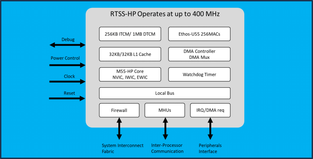
The Cortex-M55 in the RTSS-HP can operate up to 400MHz core clock frequency. The single-cycle 256KB Instruction Tightly Coupled Memory (ITCM) and 1MB Data Tightly Coupled Memory (DTCM) enable a highly deterministic, high-performance execution environment capable of running tight control loops with minimum jitter. The RTSS-HP also has its own Ethos-U55 microNPU ML accelerator with capacity of 256 MACs. The faster clock frequency, the larger TCM capacity and number of MAC/s in the RTSS-HP provide resources for implementation of advanced neural networks and faster, more accurate inference execution.
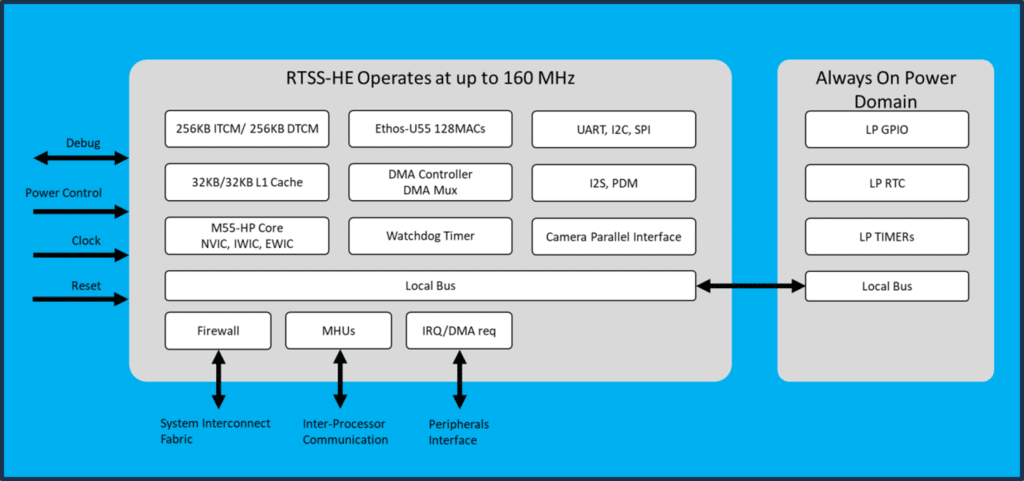
The implementation of the Cortex-M55 in the RTSS-HE is optimized for low current consumption while running up to 160MHz, and extreme low leakage current while in Standby and Stop modes. This Cortex-M55 is equipped with 256KB ITCM and 256KB DTCM for fast single-cycle memory access. The RTSS-HE resides in its own power domain and can operate standalone with minimum dependency on the other subsystems. Both the ITCM and DTCM contents can be optionally retained by a dedicated back-up power rail when the entire RTSS-HE power domain is powered off, enabling rapid wakeup. The RTSS-HE has a set of low power peripherals that can serve as a wakeup source and to support ultra-low power application requirements. The Ethos-U55 microNPU includes 128 MACs and can be used for Machine-Learning (ML)- based applications such as keyword spotting, image classification, anomaly detection, failure prediction, environmental sensing, and gesture recognition.
Shared Memory
The Ensemble family devices integrate large amounts of SRAM distributed across multiple SRAM blocks having different performance, bandwidth, and power consumption. This is done to enable users with full flexibility to partition the memory among the various execution domains based on the needs of their application.
The different types of memory blocks and their characteristics are described in the table below:
| Shared SRAM | The bulk of the SRAM is split between two blocks – SRAM0 and SRAM1. They are shared with all CPU cores. This enables the concurrent access to the memories from different execution domains. |
| Backup SRAM | The backup SRAM resides in a power domain powered by the VBAT power rail. This SRAM can be used to retain the system state needed to control different system wakeup scenarios. The backup SRAM is 4KB and can only hold data. The CPU cores cannot execute code from it. |
| Non-Volatile Memory (NVM) | The Ensemble family devices use non-volatile storage based on magneto resistive RAM (MRAM) technology. Unlike traditional flash it allows fine-grained programming of memory sectors which are only 4 words (16 bytes) in size. Applications can program (write) the MRAM simply by writing four 32-bit sequential words to the MRAM. Updates to the MRAM occur in blocks of 4 words. The MRAM programming procedure is controlled by a dedicated HW state machine that is transparent to the CPU cores. |
| External Memory | The on-chip memory capacity can be expanded through one or two high-performance Octal SPI interfaces (OSPI). OSPI supports an Execute-in-Place (XIP) mode of operation that maps the flash memory content to an address region. When a bus master requests a read operation from an address in this region, the OSPI interface translates it to a series of transactions with the external flash device and returns the result as if the read operation takes place from internal memory. This makes the access to OSPI flash transparent to the CPU cores. The OSPI peripheral also supports HyperBus protocol enabling the expansion of on-chip RAM. Like with the XIP mode of operation, read and write bus operations are translated to HyperBus commands transparently to the bus master originating the transaction. Since adding external flash memory through OSPI exposes the data being transferred, the devices feature an AES-128 hardware decryption module on the data path between the OSPI peripheral and the system interconnect. The users can install their own AES key intended to decrypt the content of the external memory on the fly. |
| External Mass Storage | External mass storage can be added through an SD/MMC controller. It supports a 4-bit data interface to external SD/MMC cards as well as an 8-bit interface to embedded MMC modules. Alternatively, the USB controller can be configured to operate in Host mode. This way, the storage capacity can be expanded using an external USB flash drive or other mass storage device. |
| Cache Memory | The cache memories accelerate the performance of the CPU cores in the APSS and RTSS execution domains. Devices with dual Cortex-A32 cores each have 32KB L1 instruction and data cache running at up to 800MHz. They share the common L2 cache which is 512KB and is running at up to 400MHz. The single core devices still utilize the full 512LB L2 cache. The Cortex-M55 cores in the RTSS execution domains have 32KB L1 instruction and data caches that are used only when accessing memory outside of the ITCM or the DTCM. |
| Tightly Coupled Memory | The HP-RTSS and HE-RTSS feature Tightly Coupled Memories (TCM) providing high-bandwidth, deterministic, single cycle access by the CPU. The TCM is split between Instruction and Data segments, each having a dedicated bus enabling their simultaneous access. The ITCM is always mapped at the local address 0x00000000 of the Cortex-M55 address space and the DTCM is mapped at local address 0x20000000. In addition, the TCMs are mapped into the global address space so that these TCM memories may be shared with the other CPU cores. The TCM memories and their corresponding address regions are described in a table below. |
The full address map is Ensemble series-specific and device-specific. Please refer to the product datasheet for detailed information for specific devices.
The table below describes the global address map from the perspective of the different application sub- systems in an of an Ensemble E7 device, for example.

The fragmented SRAM memory map can be consolidated by the MMU configuration in the APSS so that it appears as a contiguous region. The Ensemble family devices feature Firewalls that secure transactions between master and slave ports across the main interconnect fabric. The Firewalls connecting the bus masters in the RTSS-HP and RTSS-HE domains can do address translation of all read and write transactions. Like the MMU in the Cortex-A32 cores, this feature allows the Cortex-M55 CPUs or the Ethos-U55 micro-NPUs to view fragmented SRAM blocks as a single SRAM region. Please see the Conductor Tool User Guide for examples of memory configurations for the Firewalls.

The Firewalls are TrustZone-aware and perform the role of a Memory Protection Controller for each of the shared SRAM blocks. In addition to protecting secure regions from non-secure transactions, the Firewalls can filter transactions based on specific bus master IDs. This way, applications running on the different subsystems can have private secure memory regions carved out of the globally accessible shared memory.
Access to memories and shared peripherals is restricted based on the current Security Life Cycle State (LCS) and the FW configuration. When in the LCS=Development state, the Firewalls default to an Open configuration where any CPU core can access any of the memories or peripherals in the Global Address map. When in LCS=Secure state, the Firewall defaults to a Closed configuration and the CPU core cannot access any of the Global Address map without the firewalls being explicitly configured. When the life cycle of the device is advanced to the secure state, the association between memories/ peripherals and subsystems is configured by the Secure Enclave according to the system configuration specified by the Conductor tool and in response to runtime application requests.
Shared Peripherals Integration
The Ensemble family devices integrate a rich set of peripherals, such as communication interfaces, memory expansion interfaces, display and camera controllers, timers, audio, analog functions, and digital I/Os. Alif’s system architecture is designed such that peripherals are sharable between the different subsystems and are accessible in the Global Address Map. This is achieved using the following components:
• Interrupt Router – configures which subsystem will be receiving the interrupt requests coming from the shared peripherals.
• Event Router / DMA Multiplexor – configures which DMA unit and corresponding channel will be receiving the requests coming from the shared peripherals.
• Clock Generation Controller – configures which of the peripherals have their clocks gated for reducing the active power consumption. In addition, it configures the clock sources and clock dividers required to meet different communication protocol specifications.
• Firewalls – configure the security policy enabling access to specific bus masters and are controlled by the Secure Enclave. The Firewalls perform the role of a TrustZone-compliant Peripheral Protection Controller.

Interrupt Requests Routing
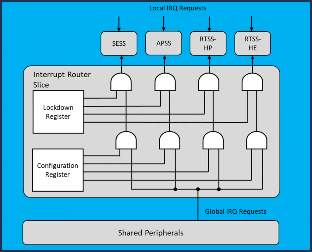
The association between interrupt requests and the interrupt controllers in the individual subsystems is configurable at run time. This function is facilitated by dedicated Interrupt Router channels with the following structure:
The diagram describes how each interrupt request is distributed to the different device subsystems. The Configuration and the Lockdown registers enable different use cases including one-to-many and one-to-one associations based on the peripheral specifics and the application needs.
In the secure state of operation, the control of the Lockdown and the Configuration registers is only accessible to the Secure Enclave. Applications request setting the Configuration register when they want to allocate a peripheral for use by invoking a Secure Enclave service.
Figure 9 Interrupt Request Distributions, Alif Ensemble E1-E7
Events Routing / DMA Requests Multiplexing

The Ensemble family devices have multiple DMA controllers intended to off-load the processor data movement tasks. High-speed peripherals such as Ethernet, USB and SD/MMC have their own dedicated DMA controllers.
The general-purpose DMA controllers (DMA0, 1 and 2) have 32 channels that can be served by 8 independent threads. They run at the same priority using round-robin scheduling. The threads can be configured as Secure or Non-Secure in compliance with the TrustZone technology.
Figure 10 General-Purpose DMA Controllers, Alif Semiconductor Microcontrollers
DMA0 expands the 32 available channels with a dedicated multiplexor called the Event Router, that exposes the available DMA channels to 128 different peripherals events. These events can include requests from peripherals such as UART or I2S as well as GPIO transitions or Timer outputs. The first 16 multiplexed DMA0 requests are also routed as input triggers to the Universal Timer. This mechanism enables the implementation of complex state machines involving the use of peripheral or time-based events that trigger data transfers and / or timer triggers.
The DMA0 controller is available for use by any of the processing subsystems. Its interrupt request lines (one for each of the 32 channels) are shared through the Interrupt Router.
DMA1 and DMA2 are dedicated for use in RTSS-HP and RTSS-HE respectively. They inherit the bus Master ID of the subsystem that hosts them so that they can access the different system resources on behalf of the associated CPU core.
Peripherals Security
In the Secure state, the access to the peripheral registers is controlled by Firewalls (similarly to the access control of the shared memory regions). The Firewalls perform the role of Peripheral Protection Controller described in the TrustZone documentation. The peripheral protection is set by the Secure Enclave in response to Application Requests to assume control over specific peripherals. This is done by preventing unauthorized access – excluding the transactions with invalid Master ID and NS side signal. Peripherals in the Ensemble family devices are designed to support low-power operation and to minimize energy consumption when not in use. Each peripheral instance has a clock gating circuit controlled by dedicated register bits. The clock gating control has two register stages – one controlled by the applications subsystems and another by the Secure Enclave.
Ensemble family devices use a pin multiplexing scheme, as the number of peripherals with interface signals can exceed the number of available pins on the device package. The pin multiplexor enables the selection of up to eight different functions per pin. In the secure state, the pin-multiplexing is only possible by dedicated service requests executed by the Secure Enclave.
System Control
Ensemble family devices integrate multiple application sub-systems, capable of simultaneously executing different embedded applications independently. These embedded applications require mechanisms to let them communicate with one another. The Message Handling Units (MHU) and the Hardware Semaphores (HWSEM) described below address the need for communication and synchronization in multi-core systems.
Inter-Process Communication with Message Handling Units
MHUs provide interrupt-driven communication between two subsystems. They support the crossing of power and clock domains. A MHU is a one-direction, peer-to-peer communication mechanism. The communication channel is represented by a 32-bit register which can be used to pass a single-word message or 32 single-bit messages. The interpretation of the data content is protocol-specific.
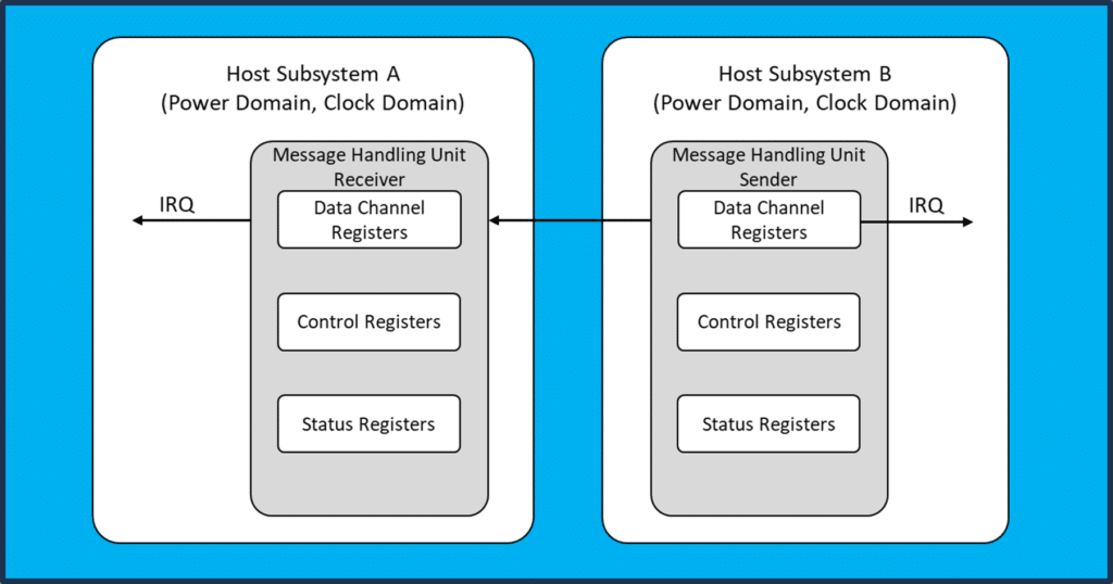
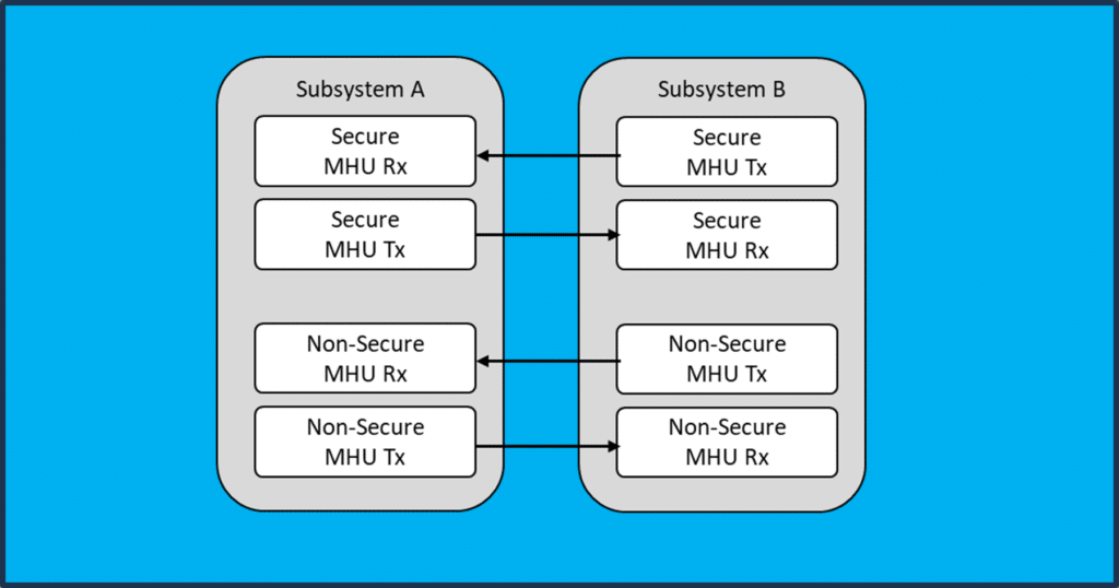
Ensemble family devices use two pairs of MHUs to support bi-directional Inter-Process Communications (IPC) between processing elements. For compliance with the TrustZone technology, the number of MHUs is doubled – enabling dedicated Secure and Non-Secure channels. In general, the IPC mechanism between any two subsystems is based on eight MHU instances organized in two full duplex channels as shown on the diagram to the left.
Figure 12 TrustZone-Compliant Use of MHUs, Alif Semiconductor Microcontrollers
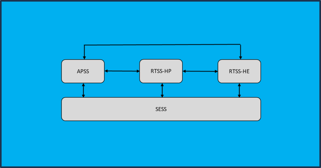
Ensemble family devices integrate four subsystems having the following IPC topology:
Figure 13 Inter-Process Communication (IPC) Topology, Alif Ensemble E5-E7 Devices

MHUs can support various transport protocols. The figure to the left describes a simple “Doorbell” protocol that uses the Receiver interrupt only to send an optional payload.
Figure 14 MHU Transport Protocol Example, Alif Semiconductor Microcontrollers
Inter-Process Synchronization with Hardware Semaphores
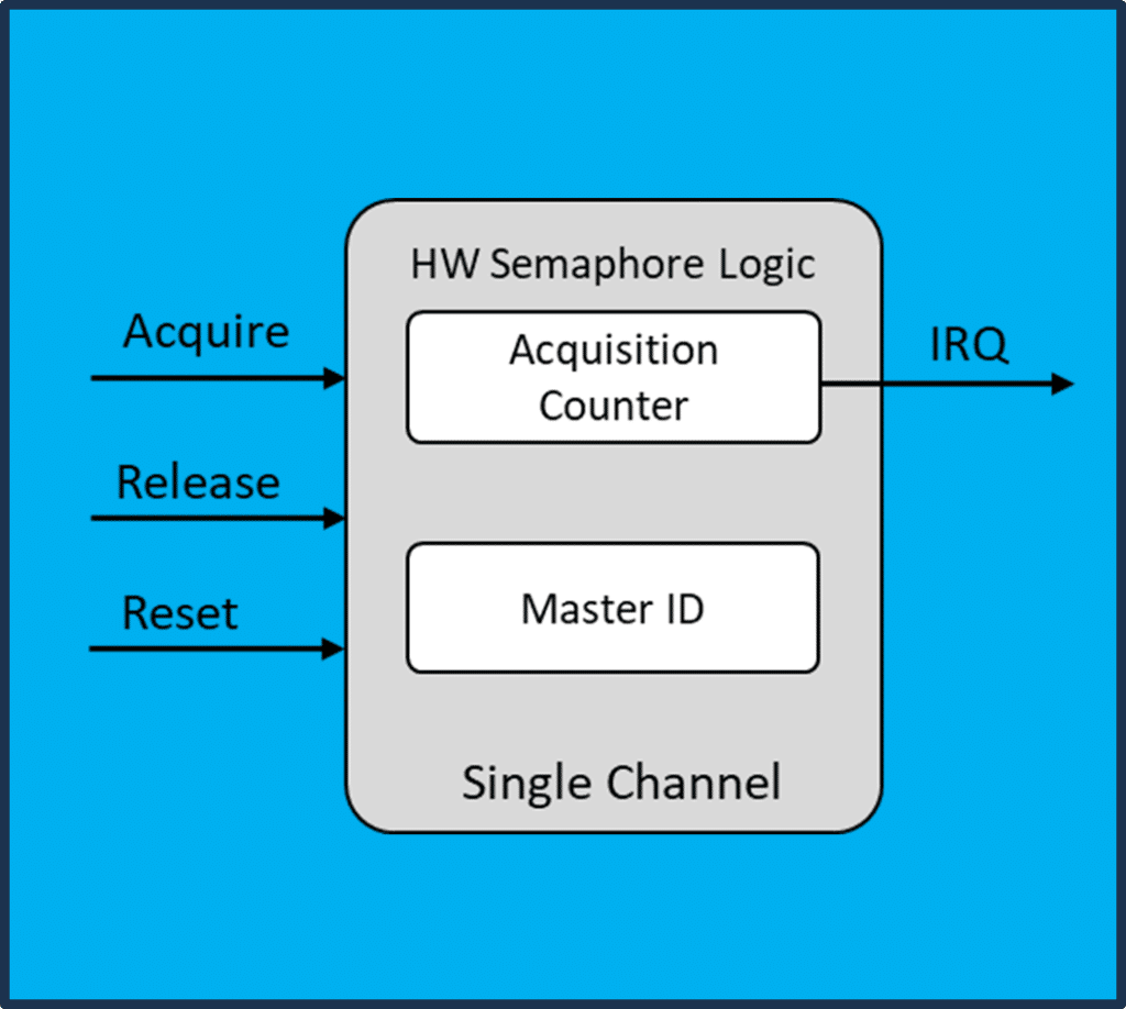
The Hardware Semaphore (HWSEM) addresses the need to synchronize the access to shared resources (memory or peripherals) by two or more independent processing elements. The device includes Hardware Semaphores operating like the counting semaphores found in most operating systems that support preemptive multi-threading. The figure to the right represents the simplified structure of a HWSEM instance.
HWSEMs perform atomic operations, serializing the concurrent requests from different bus masters. This is achieved by register read/write operations resulting in counting the times the semaphore is acquired and released by specific bus Master. A HWSEM will refuse acquisition requests from other bus Masters until the HWSEM is released. Once the acquisition counter reaches zero, the HWSEM release is signaled by an interrupt request. The processors waiting to acquire the semaphore can handle this IRQ by initiating a new acquisition request.
Figure 15 Simplified Structure of Hardware Semaphore (HWSEM), Alif Semiconductor Microcontrollers
16 instances of the HWSEM are included among the shared peripherals. Their interrupt requests are shared with all subsystems through the Interrupt Router as shown on the diagram below:

System Startup & Control
Boot Process
The Secure Enclave subsystem performs the role of device System & Security Supervisor. After reset, the SESS is the only core that starts execution, all other subsystem application cores are held in a wait state until the SE releases them. The SESS first initializes the device and sets up the security policies and then performs a boot / secure boot for the other subsystems. Once the boot process is complete, the Secure Enclave offers runtime services for security, crypto and power management AiPM functions.
The SE enables the end-product developer to have complete control of the boot sequence using a data structure located at the top address (last 16 bytes) of the developer’s MRAM area called the ATOC (Application Table of Contents). The ATOC contains configuration information used by the SE to initialize the device prior to any application core being booted. Items like the Pin Mux, System Clock configuration and Fire Wall settings may be configured. The ATOC also specifies which cores are to be booted, from what memory address, in what order, and specifies the security attributes of the boot image (signed, encrypted, etc.). Please see the SE Tools Users Guide for more information on how to create and program an ATOC and application boot images into the MRAM of the device.
If the device is in the Secure Life Cycle state, then the ATOC is required to facilitate the secure boot process. Else if the device is in the Development Life Cycle state (i.e. Not Secure), then the ATOC is optional. When no ATOC is present at the top of MRAM, the SE will start the RTSS-HE core using the following procedure.
• If the beginning of MRAM (address 0x0) contains a valid code image (Interrupt vector table), then the SE will boot the RTSS-HE from the beginning of MRAM (address 0x0).
• Else if there is no valid code image at the beginning of MRAM, then the SE will load a debug stub into the ITCM of the RTSS-HE and start execution of the Debug stub so that the user can easily connect a debugger to the RTSS-HE core and control it as needed. This process enables the user to easily program code into the beginning of MRAM and the device will boot this code using the RTSS-HE
An Ensemble device may be powered up by applying power to the device (Normal Boot Process) or the device can power up from Stop mode via wake-up events (Wake-up Boot Process). These wake-up events may be configured by the application code to boot up certain subsystems with various system configuration settings. These are specified as part of the AiPM functionality for the device and are controlled by the SE during wake-up events.
Lastly, the SE provides a UART interface named SEUART that enables SE Maintenance tools to connect to the device and perform various recovery or maintenance functions on the device during development. The Maintenance tool enables users to display device settings, program MRAM, display debug information, and to provision end-product developer credentials into the device when needed. Please see the SE Tools User Guide for more information on these tools which will assist in development.
The device Non-Secure boot process is outlined in the flow diagram below:

Application Deployment
Ensemble family devices feature many shared peripherals and up to 13.5 MB of SRAM and up to 5.5MB of non-volatile MRAM, either of these memories can store application code and/or data. Since Ensemble devices have multiple cores, it is recommended that the user’s selection of SRAM and MRAM memory map layout is defined during the development process detailing which MCU cores will have dedicated access or shared access to sections of these memories and individual peripherals. The online Alif Conductor tool is designed to assist with this process. The Conductor tool also assists in configuring device system clocks and the peripheral Pin Mux settings. Please see the Alif Conductor User Guide for more information.
The Alif Conductor tool saves a user’s device configuration information into a file that can be downloaded for use with the Alif ATOC tools to create an ATOC image to be written to MRAM which governs device-level configuration, secure boot, and CPU boot sequence at run time.
Note: The Application code itself is developed using standard MCU development tools / IDE tools. The resulting executable image from the standard MCU build process can be programmed into MRAM where the application CPU cores will boot them. Standard debug tools may also be used in the development process to debug software and program the device. Please see the Getting Started Application Notes for more information on the development process.
Summary
This document introduced the top-level system architecture of the Ensemble family devices and their programming models. It includes descriptions of the various software execution environments, memories, peripherals, and the connections between them. Finally, there is an overview of the boot process, security features, and inter-process communication.
Detailed device specifications are provided in the respective device Datasheets. For further detailed information about specific hardware components (CPUs, NPUs, memories, peripherals, their register settings, etc.) please refer to the products’ Hardware Reference Manuals. For further information about the devices’ software programming model, software concepts, APIs, etc., please refer to the product Software Reference Manual.