

Introduction
The Ensemble® family of processors from Alif Semiconductor® are designed to be energy efficient with an architecture capable of deployment in battery powered environments. Alif processors use energy efficient cores capable of waking up to perform tasks and sleeping to save energy. This contrasts with high powered devices that are always on and must stay plugged in to a power source.
Alif’s multicore processors are equipped with high-performance and high-efficiency cores separated by operating regions which then clock gate or power off. Industry leading battery life can be achieved by employing power saving features such as running at high or low frequencies, clock gating as necessary, powering off unused regions, and sleeping for extended periods. The sum of this comprises Alif’s Autonomous Intelligent Power Management (aiPM™) technology that essentially powers on only what’s needed, when needed, in the most efficient manner. This white paper will detail the power management architecture of the device and will describe the power-saving features available to use in the design of your application.
The Ensemble family scales from single-core microcontrollers to multi-core fusion processors. The fusion processors combine up to two Cortex-M55 microcontroller cores, two Cortex®-A32 microprocessor cores, and two Arm Ethos®-U55 microNPUs.
Power Saving Features Overview
Operating Regions
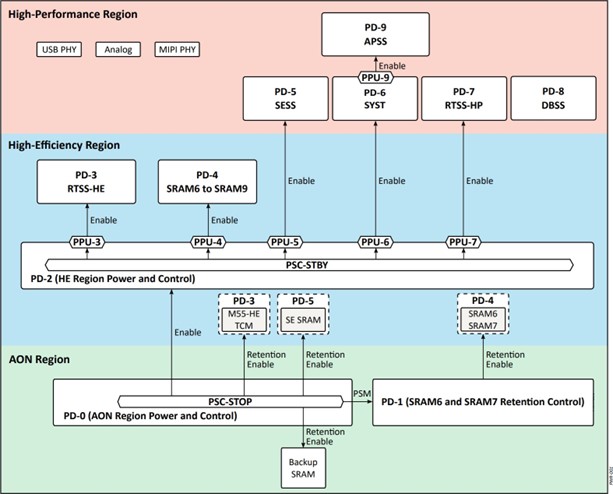
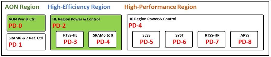
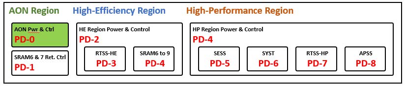
All sub-components of the Ensemble processor are encapsulated in one of three operating regions: High-Performance, High Efficiency, and AON (always-on).
High-Performance Region: The highest clocked cores and memories will reside in the High-Performance Region since they can run at higher frequencies up to 400MHz to 800MHz while running on the PLL. Within the High-Performance Region there are two processing subsystems of interest:
- APSS: two Cortex-A32 microprocessor cores (up to 800 MHz)
- RTSS-HP: Arm Cortex-M55 MCU and Ethos-U55 microNPU (up to 400 MHz)
Also within the High-Performance region is PD-6, the SYST power domain. This subsystem contains many of the central device resources shared between the processing subsystems. These shared resources are:
- Main system interconnect facilitating data movement between subsystems
- Two SRAM memory banks of up to 4 MB + 2.5 MB
- Non-volatile memory: MRAM on-chip, OSPI and SDMMC off-chip
- System peripherals (excluding LP- peripherals)
High-Efficiency Region: This region is comprised of lower leakage transistors on the die and is clocked at a lower frequency than the High-Performance region. The High-Efficiency region can be used for simpler computation tasks, machine learning tasks, and connectivity services while the High-Performance region is powered down. Developers can choose to perform many tasks in this region, using lower power and lower frequency components, without needing to wake the High-Performance Region. Processing subsystems of the High-Efficiency Region are as follows:
- RTSS-HE: Arm Cortex-M55 MCU and Ethos-U55 microNPU (up to 160 MHz)
Other resources within the High-Efficiency region include:
- LPSPI, LPI2S, LPPDM, LPCPI peripherals within PD-3 RTSS-HE
- LPUART and LPI2C peripherals within PD-2 STBY
Battery Always On Region (AON): This contains the shared RTC, LPTIMER, LPGPIO, LPCMP, and 4KB of Backup Memory. The region is always running when a battery or sustained power source is connected to the VDD_BATT supply. The processor can be placed in an extreme power saving mode, called STOP Mode, where the High-Performance and High-Efficiency Region are powered off leaving only the AON Region.
The operating regions are summarized below in Table 1 Processor Operating Regions. Note that each processing subsystem may contain memories and peripherals within it, i.e., local resources, that are separately clocked and powered from the centrally held shared resources in PD-6 SYST. Please refer to the “Device Resources per Power Domain” section of the device datasheet for more information on the operating regions, subsystems, and power domains.
| Battery Always-On Region Lowest Frequency Lowest Leakage | High-Efficiency Region Lower Frequency Lower Leakage | High-Performance Region Higher Frequencies Higher Leakage |
| Power Domains 0 and 1 | Power Domains 2, 3, 4 | Power Domains: 5-9 |
CPU States
Embedded systems are often interrupt driven, meaning incoming signals from the system are used to notify the CPU when data is ready or that a task should be started. Then, when the task is complete, the CPU enters an idle loop waiting for the next interrupt. In a battery powered system, developers avoid idle loops which consume unnecessary energy so processors will instead clock gate or power off the CPU in between tasks. In Alif processors, each processing subsystem’s CPU can do the same by operating in one of one of three CPU States: RUN, SLEEP, or OFF. Developers can choose between these states, described in Table 2 CPU States Summary, and use them to affect the power consumption of the device.
| CPU State | Description |
| RUN | When a CPU core’s clock is running, typically executing code. |
| SLEEP | When a CPU core’s clock gated and can quickly resume. |
| OFF | When a CPU core and its subsystem are powered down. |
When a core in a processing subsystem is running and executing code it is in the RUN State. Any code execution, while loops or “no-op” instructions will keep the core’s clock running. Power consumption is highest in the RUN State. Developers can choose to stay in this state for continuous polling or for time critical applications where application response should be as quick as possible. In a power sensitive application, a core can reduce its power draw compared to the RUN State by entering the SLEEP State where its core clock will be stopped. During the SLEEP State, the CPU’s core clock will be stopped. Developers can choose this state to stop all code execution until an interrupt event wakes the core again. Since no power is lost in the subsystem, the core has retained its context and can resume the RUN State quickly.
Developers interested in more significant power savings will have a core and its processing subsystem further placed in the OFF State. When the CPU core is powered off it eliminates the leakage power that is otherwise still present in the SLEEP State. In addition to the CPU core, all logic in the processing subsystem loses power. This is because the CPU core cannot power off independently of its local subsystem. Any resources in the subsystem are powered off along with the CPU core, including certain LP- peripherals in the case of PD-3 RTSS-HE. Details are in Table 3 Local Resources within each RTSS.
| Processing Subsystem | Local Resources |
| RTSS-HP | 1.25MB TCM, Ethos-U55 256 MAC, DMA1 instance, M55-HP (M55 core, L1/L2 Cache, NVIC), Watchdog Timer |
| RTSS-HE | 0.50MB TCM, Ethos-U55 128 MAC, DMA2 instance M55-HE (M55 core, L1/L2 cache, NVIC), Watchdog Timer, LPSPI, LPI2S, LPPDM, LPCAMERA, and APB bus used to access the VBAT domain LPRTC, LPGPIO, and LPTIMER |
All processing subsystems can change between the CPU States listed above and they can do so independently of each other. For example, one RTSS may be off while the other RTSS is awake capturing sensor data. The Secure Enclave Subsystem (SESS) maintains its own sleep and wake cycles. Its behavior is dictated by a combination of Alif System Software and any configuration input by user software. Generally, developers should aim to architect their applications to minimize time spent at the highest states and allow for power-saving sleep cycles in between tasks.
SYST States
Many of the Ensemble processors’ shared resources and system interconnect reside in a power domain called PD-6 SYST. The default device configuration leaves SYST in the always-on state. This allows applications to configure and utilize shared resources such as SRAM0/1 and system peripherals without special considerations. As long as PD-6 SYST remains powered on then the contents of SRAM0/1 will be retained and the configurations on system peripherals will not be lost. Applications which are using the system peripherals will want to use SYST in the always-on state.
If the application does not require the retention of SRAM0/1 memory and does not require retention of system peripherals (because it is using local resources like TCM and LP- peripherals) then PD-6 SYST can be configured to use the dynamic off state. Any transactions which cross between subsystems will cause PD-6 SYST to power on and service that transaction, but it will power off as soon as the data movement is completed. Significant savings in dynamic power and leakage power can be achieved by using SYST in the dynamic-off state.
MCU States
As mentioned, the processing subsystems are meant to independently change CPU States without coordination with each other. Beyond these CPU States, Alif has defined additional SoC Power Modes that affect the central device resources shared between each processing subsystem. The overall SoC is in GO Mode as long as one processing subsystem is in the RUN or SLEEP State. In GO Mode all central device resources (clocks, memories, peripherals) are available for use by any of the processing subsystems. The device will stay in GO Mode for as long as any shared resource is being utilized.
It is up to the SESS to determine when to change SoC Power Modes. When all processing subsystems are off and shared resources are not utilized then the SESS will be able to transition the SoC to STANDBY or STOP Mode.
| Device Power Mode | Wake-Up Peripherals | |
| GO | One or more Processing Subsystems are in RUN or SLEEP state | All |
| READY | All processing subsystems are in SLEEP state. | All |
| IDLE | All processing subsystems are in OFF state. | All |
| STANDBY | All Processing Subsystems and shared resources in the High-Performance region are powered down. | All GPIO, LPUART, LPI2C, plus STOP Mode wake-up peripherals |
| STOP | All Processing Subsystems and shared resources in the High-Performance and High-Efficiency regions are powered down. Few peripherals remain with extremely low leakage. | LPTIMER, LPCMP, LPRTC, and LPGPIO |
Power Management Unit
A Power Management Unit (PMU) in the processor controls the internal LDOs, DCDC, and clock generation. It is responsible for enabling or disabling the resources depending on the SoC Power Mode.
| Power Mode | Clock Availability | DCDC Status |
| GO | All Clocks and PLL enabled | DCDC: full power |
| STANDBY | LFXO or LFRC (32,768 Hz) and HFRC (38.4 MHz or 76.8 MHz) | DCDC: efficiency |
| STOP | LFXO or LFRC (32,768 Hz) only | DCDC: Off |
Retention Memory – RTSS-HE TCM
For the RTSS-HE, its 512KB TCM supports an option to be retained while the RTSS-HE is powered off. Normally, turning off either RTSS results in a power loss to the TCM and its contents will be erased. In the case of the RTSS-HE an option is available to keep its TCM powered on separately. Enabling this feature increases the static current of the device in the low power modes but it allows for increased flexibility in applications using the low power modes. They can benefit by keeping code or data retained in memory between power cycles. The tradeoff depends on multiple factors. A memory fill at every wake cycle takes time and energy if the TCM is not retained. On the other hand, increased static current should be accounted for when the TCM is retained.
Current consumption at 3.3V: 2.3 μA to retain 256KB or 4.7 μA to retain 512KB of RTSS-HE TCM
Retention Memory – 4KB Backup SRAM
There is 4KB of SRAM in PD-0 which can be used for saving critical information before entering low power STANDBY or STOP Mode. This memory will stay retained and its contents will never clear if a valid voltage is maintained on the VDD_BATT supply.
Current consumption at 3.3V: 50 nA to retain Backup RAM
Retention Memory – Secure Enclave SRAM
The Secure Enclave Subsystem (SESS) is an isolated security processor and system controller. It performs initial system configuration after reset and securely boots the other processing subsystems. The stored location for the Secure Enclave (SE) firmware is in a secured part of MRAM. When the SESS is powered on the SE Firmware is verified and copied to the Secure Enclave SRAM. Loading the firmware from MRAM includes certain time-consuming procedures that can be eliminated by retaining the SE firmware in SRAM throughout the power-saving modes. Upon wakeup, the SE firmware will already be in SRAM so that the response time to wakeup requests is significantly improved.
Estimate: 1.8 uA to retain 256KB of Secure Enclave SRAM
Impact: 40 ms estimated improvement in the wakeup response time from STOP Mode
Selectable Clock Frequencies
Much of the processor runs at high frequencies centrally sourced from the device PLL. The output frequency of this PLL remains fixed and programmable clock dividers reduce the frequency for the device subsystems. Applications may choose to run at a high frequency where it is more efficient to complete a task quickly and immediately enter a sleep cycle. Other applications may not have the flexibility and must stay awake longer. These mux options let application cores run at reduced clock frequencies to minimize power consumption and extend battery life.
CPU States and Power Modes Detail
CPU RUN State
A processor subsystem is in the CPU RUN State any time the processor core is fetching and executing instructions, including while executing the “no-op” instruction, while in an empty for(;;) loop, or in a while(1) loop. This means power and clocks to the processor core, local memories, and local resources are all enabled. The rest of the processor, other subsystems, shared peripherals, and shared memory are available as well. Dynamic power and static power within the processor subsystem are highest in this mode. An example of this mode is shown in Figure 2 below.

While the CPU is in the RUN State, the best way to save power is via clock frequency scaling. When reducing the main clock to the APSS or RTSS this will help to reduce dynamic power within the processing subsystem. The clocks to the APSS or RTSS are independent from other subsystems and only affect the CPU cores and local resources to the subsystem. Peripherals in PD-6 SYST are clocked from other sources and can continue to run without being affected by APSS or RTSS clock changes. Clocks within PD-6 SYST are also adjustable and can be reduced for power saving purposes without affecting APSS or RTSS clock sources.
CPU SLEEP State
Entering SLEEP State is done by a processor core executing the WFI or WFE instruction. In the SLEEP State, a processor core will clock gate, but local resources within the subsystem and shared resources in other subsystems will continue operating. Local and shared resources may then generate interrupts to resume CPU RUN State on the processor. There is no limit to interrupt availability when entering CPU SLEEP State; all interrupt sources in PD-6 SYST will be available to wake any processing subsystem.
Due to the clock gating of the processor core, dynamic power within the processor subsystem is reduced in this mode relative to the CPU RUN State. Power is retained for the processor core and its local memories, however, so no application state information is ever lost making this mode the fastest to resume operation via interrupt. Peripherals in PD-6 SYST are clocked from other sources and can continue to run therefore power consumption caused by any activity in the shared resources domain remains present.

CPU OFF State
If the application allows, a processor subsystem may be placed in the CPU OFF State where the processor core, local memories, and local resources are all disabled and powered off. Resuming CPU RUN State via hardware interrupt is possible using the MHU or the LP- peripherals listed in Table 6 OFF State Wakeup Sources.
The example in Figure 4 below shows an example of some processing systems being OFF and some being in SLEEP, demonstrating that not all processing systems have to be in the same state.

When a processor subsystem powers off it will do so independently of other subsystems. Other subsystems may be active but dynamic power and static power within the local processor subsystem are eliminated in CPU OFF State. Optionally, at the expense of increased static power, the local memories can be retained in RTSS-HE only.
Wakeup Sources in CPU OFF State
These wakeup sources must be configured and enabled, and a CPU reset vector must be set before the RTSS enters the CPU Off state. Upon peripheral interrupt, the RTSS will power on and begin executing application code from its reset vector. While the RTSS is off the CPU core will lose current application state information, so it is important to save application-specific information in retainable memory regions such as the 4KB Backup SRAM.
| Interrupt Source | Destination |
| LPI2C | RTSS-HE |
| LPUART | RTSS-HE |
| LPCMP | RTSS-HE and RTSS-HP |
| LPGPIO[7:0] | RTSS-HE and RTSS-HP |
| LPRTC | RTSS-HE and RTSS-HP |
| LPTIMER[3:0] | RTSS-HE and RTSS-HP |
| MHU IRQs | RTSS-HE and RTSS-HP |
SoC STANDBY Mode
When the High-Efficiency Region is on, and all higher numbered domains are off (PD-3 and up), the device is in STANDBY Mode. Using STANDBY Mode makes available some clocks and modules that are not available in STOP Mode. The cost is higher static power relative to STOP Mode. The clocks and modules enabled by this mode are in High-Efficiency Domain (PD-2) shown in the Power Domains Table. To wake up other subsystems a request from the RTSS-HE can be made to the SESS. Then the SESS will be responsible for waking that core.
Current consumption at 3.3V: 65 µA
Wakeup Sources in STANDBY Mode
While in STANDBY Mode, these modules can generate interrupts to wake the RTSS-HE. Note: When the RTSS-HE wakes up during STANDBY Mode this will not automatically wake up the High-Performance Region or the Shared Resources domain (PD-6). The RTSS-HE may operate in this mode executing within its TCM alone using only the peripherals within PD-3, without using any of the device’s shared resources. It can then go back to STANDBY Mode for the next sleep cycle. If other cores or peripherals are needed, then it can make a request to the SESS to wake the system out of STANDBY Mode.
| Interrupt Source | Destination |
| LPI2C | RTSS-HE |
| LPUART | RTSS-HE |
| LPCMP | RTSS-HE |
| LPGPIO[7:0] | RTSS-HE |
| LPRTC | RTSS-HE |
| LPTIMER[3:0] | RTSS-HE |
SoC STOP Mode
When the AON Region is on, and all other regions are off, the device is in STOP Mode. The infrastructure for routing interrupts to the subsystems is not available anymore. Instead, any wake requests from the AON Region will wake the SESS. From there the SESS will wake one of the processor subsystems which requested entering STOP Mode.
Current consumption at 3.3V: 1.6 µA with 4KB Backup RAM retention
Wakeup Sources in STOP Mode
A selection of LP- modules can be enabled before entering STOP Mode. These modules can then generate interrupts to wake the device. It is the application’s responsibility the configure the below modules for generating an interrupt. After which the application will request STOP Mode through a SE API call.
| Interrupt Source | Destination |
| LPCMP | SESS |
| LPGPIO[7:0] | SESS |
| LPRTC | SESS |
| LPTIMER[3:0] | SESS |
Wakeup Times from Power Saving Modes
SoC Power-On-Reset
A power-on-reset occurs when power is first applied to the SoC or when the external reset pin is toggled. Hardware state machines bring up internal power supplies, ring-oscillators, and initial power domains like the Secure Enclave Subsystem (SESS). The hardware initialization completes in microseconds however this boot procedure includes an SE firmware startup process which can be slow. The SE firmware, for devices in the Secure Life-Cycle-State, must be verified for secure boot. Next, the firmware is copied to Secure Enclave SRAM adding to the boot time. After the copy, SE firmware will start. Here it will process the Application TOC and apply additional SoC configurations. Finally, the RTSS and APSS applications will be verified for secure boot, if needed, and started.
Estimate: 50 milliseconds boot time from power-on-reset to application start
SoC STOP Mode
In the most restrictive form of STOP Mode, very few SoC components remain active with only low-frequency clocks and minimal resources in PD-0 and PD-1 enabled. Resuming operation is like the power-on-reset process described above but slightly modified. A hardware initialization is completed in microseconds and the RTSS-HE is booted at this point which is then followed by the SE firmware startup process. The RTSS-HE is intentionally given a chance to wake up as early as possible while the SE
firmware startup continues separately. Initializing the PLL is a step that is skipped when resuming from STOP Mode to shorten the wakeup time and to reduce the energy consumed in cases where the PLL isn’t needed. A request can be made to the SE firmware to start the PLL if it is needed.
Estimate: 786 microseconds from an interrupt in STOP Mode to RTSS-HE application start
SoC STANDBY Mode
After entering STANDBY Mode, much of the SoC’s base hardware remains initialized, and high-frequency ring-oscillator clocks may be kept running. This common basic infrastructure resides in the High- Efficiency Domain (PD-2), and it enables wake-up requests to be routed directly to the RTSS-HE subsystem where an application on that core will need to respond. Since the hardware initialization steps are skipped, the RTSS-HE can respond to wakeups more quickly than with STOP Mode.
Estimate: 5 microseconds wakeup time from STANDBY Mode interrupt to RTSS-HE application start
Conclusion
Maximizing the time spent in STANDBY and STOP Mode is critical and will lead to a successful low-power design. To help with this, the Ensemble processor provides timers, comparators, GPIO, and other LP- peripherals that an application can use to efficiently dictate its wake and sleep cycles. When the device is asleep, aim to use the LP- peripherals to efficiently monitor and respond to the physical world. Only use the memory retention options to benefit applications that will benefit from it. Develop smart ways for applications to save their context in the RTSS-HE SRAM or the Backup SRAM and then wake up as quickly as possible. Then, when the device is awake, use the high-efficiency domain for low-level tasks, data collection, and general maintenance to sip minimal power and low frequencies. Only when needed, enable the high-performance features of the Ensemble family, such as the Ethos-U55 accelerator, Cortex-M55 with Helium DSP extensions, and high-frequency clock options. Finally, allow software to complete tasks quickly and return to sleep immediately.